Contact:TOM LIN
QQ:1511841311
Tel:00852-34604012
Fax:00852-34604018
Phone:15112297719
E-mail:linxiansheng@mallchips.com
ADD:FLAT/RM B 5/F GAYLORD COMMERCIAL BUILDING 114-118 LOCKHART ROAD HK
Industry news
Automotive MOSFETs – A Package Deal That’s Worth It
Generally, the more efficient components become the smaller, lighter, longer lasting, and cheaper the final products become, and the less likely they are to heat up. Some applications are not even possible until components reach a certain degree of efficiency. As a result, with greater efficiency comes greater demand for relevant components, providing further growth.

System Efficiency is King
Switches – usually MOSFETs – are key components that play a defining role in efficiency. Their conductivity and switching losses are critical in determining heat loss. The “figure of merit” parameter (ON resistance RDSon × gate charge Qgate) allows us to evaluate static (electrical conductivity losses) and dynamic (electrical switching losses) performance.
Tweaks for smaller figures of merit or higher efficiency in MOSFETs can be performed using semiconductor materials with superior properties such as SiC or GaN. These materials offer reduced dynamic losses by means of faster switching and lower thermal resistance compared to conventional silicon MOSFETs. This is especially true at higher voltage levels. But MOSFET systems consist of more than just a semiconductor chip. The package and connection technology also play an important role.
Reduce Power Loss by Reducing Overall Resistance
If we consider the distribution of the ohmic resistance of a MOSFET-on-chip with its contacts and package, we notice how the resistance values of package RPackage and the resistance of the die are connected in series (Figure 1).
Therefore, it is not enough to simply keep developing better and better MOSFET chips. The package technology also needs to keep pace with these optimizations. The following methods are available to achieve this:
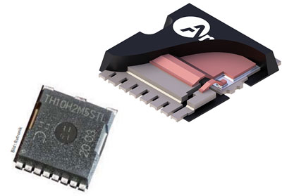
Surface contacts instead of bond wires: The larger contact and cross-section area helps reduce the thermal and electrical resistance of the package (Figures 2, 3, and 4). An extra bonus is that the strip-like form of the contact clip also reduces the parasitic inductance of the connection.
Thinner dies: Thinner dies offer two advantages. The first is that the overall electrical resistance is reduced because the length of the path of the current through the chip is reduced overall. Additionally, the channel is closer to the surface, which further reduces thermal resistance.
Source-down packages: A source-down package has the channel, where the heat loss is generated, positioned closer to the cooling surface. This provides the component with better electrical and thermal properties. Infineon has introduced the first MOSFETs with a 3.3 × 3.3 mm² PQFN package and inverted die. It refers to this technology as “source-down” technology.
Improved Usage of the Die, Thanks to Reduced Thermal Resistance
This shows how improved heat dissipation to the environment allows for greater heat loss without causing the component itself to overheat. The aforementioned surface contact of the chip helps in this regard. But there are several additional measures that can be taken.
Cooling from Above
In conventional packages, the MOSFET chip is located with the drain facing down on the metallic contact surface. This drain connector is soldered to the PCB and represents the main path for heat dissipation into the board.
However, the PCB itself has to be cooled. This is why the heat energy is often conducted to the other side of the PCB using thermal vias. The PCB and its vias add extra heat resistance on the route from the MOSFET to the environment. In this case, the rear of the PCB can be fitted with a heat sink.
However, if the cooling surface is located on the upper side of the MOSFET package, a heat sink can also be connected upon it directly. The heat resistance generated by the PCB and its vias then ceases to be a factor.
Cooling from Above and Below (Dual Side Cooling, DSC)
This special package has not yet been broadly adopted, so developers are limited in their choice of types and manufacturers and there are hardly any second sources available.
Table 1 lists the standard packages of various manufacturers and their properties. It clearly shows that the largest packages do not automatically offer the smallest thermal resistance values.
Conclusion
To allow the latest MOSFETs to fully benefit from their package advantages, manufacturers have also provided innovations in package technology. Recent dies in packages with surface contacts using copper clipping provide a remarkable improvement in electrical and thermal properties. This provides a path to smaller, lighter, longer-lasting, and cheaper applications, and may even facilitate entirely new ones.

